


Designing a PCB for SMT assembly can seem like a daunting task, but with the right approach, it can be a smooth and rewarding process. As an SMT PCB assembly supplier, I've seen firsthand the importance of getting the design right from the start. In this blog post, I'll share some tips and best practices on how to design a PCB for SMT assembly.
Understanding SMT Assembly
Before we dive into the design process, let's quickly go over what SMT (Surface Mount Technology) assembly is. SMT is a method of attaching electronic components directly to the surface of a printed circuit board (PCB). This is in contrast to through-hole technology, where components are inserted into holes drilled in the PCB. SMT offers several advantages, including smaller component size, higher component density, and better electrical performance.
Design Considerations
Component Selection
The first step in designing a PCB for SMT assembly is to select the right components. When choosing components, consider factors such as size, shape, and electrical characteristics. Make sure the components you choose are compatible with the SMT assembly process. For example, some components may require special handling or soldering techniques.
PCB Layout
The layout of your PCB is crucial for successful SMT assembly. Here are some key points to keep in mind:
- Component Placement: Place components in a logical and organized manner. Keep related components close together to minimize trace lengths and reduce signal interference. Avoid placing components too close to the edge of the PCB, as this can cause problems during assembly.
- Trace Routing: Design your traces to be as short and straight as possible. This helps to reduce signal loss and electromagnetic interference. Use appropriate trace widths and spacing to ensure proper electrical performance.
- Grounding and Power Distribution: Proper grounding and power distribution are essential for a reliable PCB design. Use a ground plane to provide a low-impedance path for electrical currents. Make sure to distribute power evenly across the PCB to avoid voltage drops.
Solder Mask and Silkscreen
The solder mask and silkscreen are important elements of your PCB design. The solder mask is a layer of material that covers the copper traces on the PCB, except for the areas where components will be soldered. This helps to prevent solder bridges and other soldering defects. The silkscreen is used to label components, provide reference designators, and add other important information to the PCB.
Design for Manufacturability (DFM)
Design for Manufacturability (DFM) is a set of guidelines and best practices that help to ensure your PCB design can be easily and cost-effectively manufactured. When designing your PCB, consider the following DFM factors:
- Component Spacing: Make sure there is enough space between components to allow for proper soldering and inspection. Follow the manufacturer's recommendations for component spacing.
- Pad Design: Design your pads to be the correct size and shape for the components you are using. Use appropriate pad sizes and shapes to ensure proper solder joint formation.
- Via Placement: Place vias (holes in the PCB that connect different layers) in a way that minimizes signal interference and ensures proper electrical performance. Avoid placing vias too close to components or traces.
Design Tools
There are several software tools available for designing PCBs. Some popular options include Eagle, Altium Designer, and KiCad. These tools offer a range of features and capabilities, from basic PCB layout to advanced simulation and analysis. Choose a tool that suits your needs and level of experience.
Design Review
Once you have completed your PCB design, it's important to conduct a thorough design review. This helps to identify any potential issues or errors before the PCB is manufactured. Here are some things to look for during the design review:
- Component Placement: Make sure all components are placed correctly and there are no conflicts or overlaps.
- Trace Routing: Check that all traces are routed correctly and there are no short circuits or open circuits.
- Solder Mask and Silkscreen: Verify that the solder mask and silkscreen are accurate and legible.
- DFM Compliance: Ensure that your design meets all DFM requirements.
Working with an SMT PCB Assembly Supplier
As an SMT PCB assembly supplier, we can provide valuable assistance throughout the design process. We can offer advice on component selection, PCB layout, and DFM. We can also help you optimize your design for cost and performance. When working with an SMT PCB assembly supplier, make sure to communicate your requirements clearly and provide all necessary information, such as component specifications and design files.

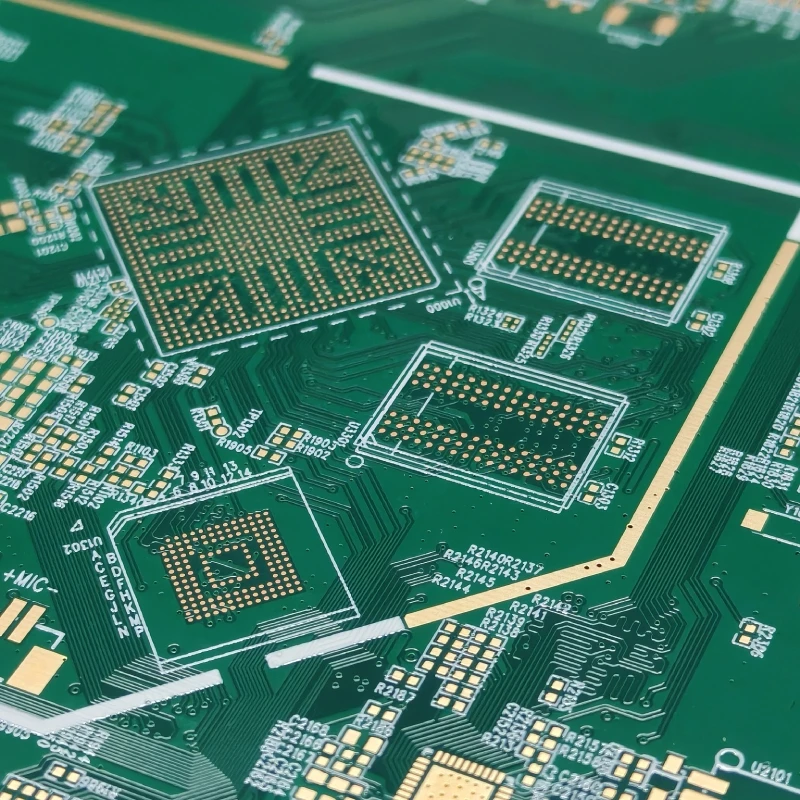
Fine Pitch SMT and Other Services
In addition to standard SMT assembly, we also offer Fine Pitch SMT and Mixed Technology PCB Assembly. Fine Pitch SMT is used for components with very small pitch sizes, which require special handling and soldering techniques. Mixed Technology PCB Assembly combines SMT and through-hole components on the same PCB. We also offer High Volume PCB Assembly for large-scale production runs.
Conclusion
Designing a PCB for SMT assembly requires careful planning and attention to detail. By following the tips and best practices outlined in this blog post, you can create a high-quality PCB that meets your requirements. If you have any questions or need assistance with your PCB design, don't hesitate to contact us. We're here to help you succeed.
References
- Printed Circuit Board Design for Manufacturability, IPC-2221A
- Surface Mount Technology Handbook, Second Edition, by Peter C. Pang
- Design for Manufacturability and Assembly, by Harry W. Oliver


