


As a seasoned provider of quick - turn PCB assembly services, I'm often asked about the minimum clearance between traces on printed circuit boards. This parameter is crucial as it significantly impacts the performance, reliability, and manufacturability of PCBs. In this blog, I'll delve into the intricacies of minimum trace clearance, exploring what it is, factors influencing it, and why it matters in quick - turn PCB assembly.
Understanding Minimum Clearance Between Traces
The minimum clearance between traces in a PCB refers to the shortest distance that should be maintained between two adjacent conductive paths on the board. This distance is typically measured in mils (thousandths of an inch) or millimeters, and it serves multiple purposes.
First and foremost, the minimum clearance helps prevent electrical interference between traces. When traces are too close together, there is an increased risk of capacitive and inductive coupling, which can lead to signal noise, crosstalk, and even circuit malfunction. By maintaining an appropriate minimum clearance, we can ensure that signals travel cleanly and accurately along their intended paths.
Secondly, minimum clearance is essential for the manufacturing process. During the PCB fabrication, traces are created using processes such as etching or plating. If the clearance between traces is too small, it becomes challenging to etch or plate the traces accurately, leading to potential shorts or open circuits. In the case of quick - turn PCB assembly, where rapid turnaround times are a priority, having a sufficient minimum clearance helps streamline the manufacturing process and reduces the risk of costly errors.

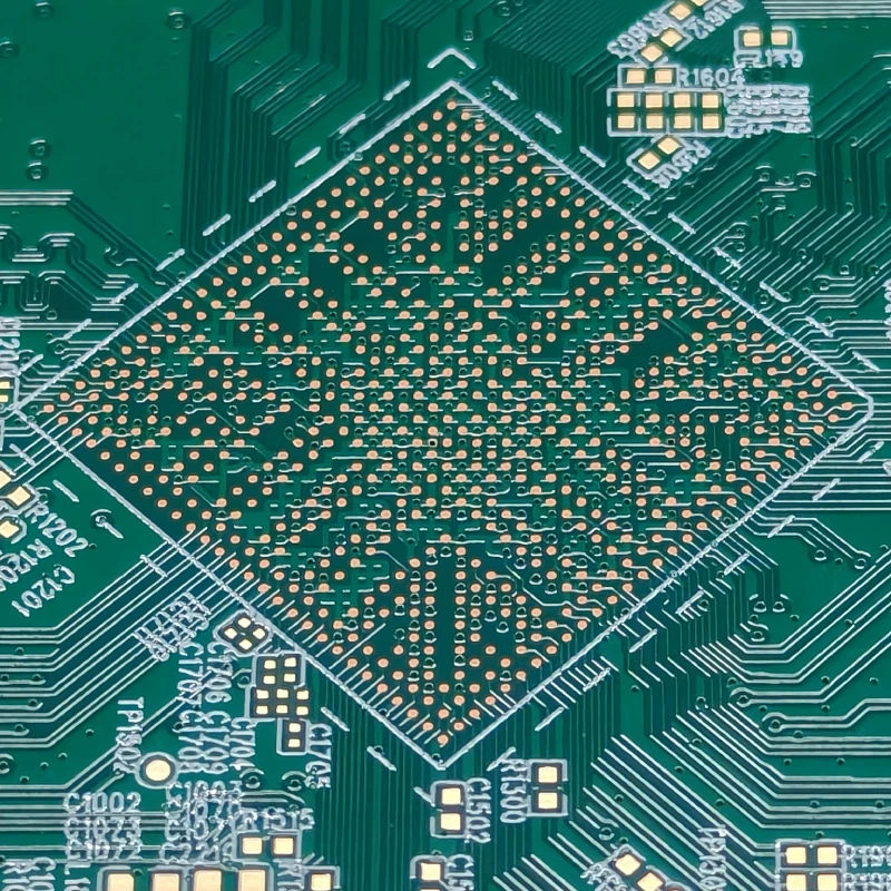
Factors Influencing Minimum Trace Clearance
Several factors come into play when determining the minimum clearance between traces in a PCB. Let's take a closer look at some of the most significant ones:
Voltage and Current
Higher voltages and currents require larger minimum clearances to prevent electrical arcing and breakdown. When a high - voltage difference exists between two adjacent traces, there is a greater likelihood of electrical discharge if the clearance is insufficient. Similarly, high - current traces generate more heat, and if the clearance is too small, the heat may not dissipate effectively, leading to overheating and potential damage to the PCB.
PCB Material and Dielectric Constant
The type of PCB material and its dielectric constant also affect the minimum trace clearance. Different materials have different electrical properties, and those with a higher dielectric constant can allow for smaller clearances between traces. However, it's essential to consider the trade - offs, as some high - dielectric - constant materials may also be more expensive or difficult to work with in the manufacturing process.
Signal Frequency
In high - frequency applications, the minimum trace clearance becomes even more critical. At high frequencies, signals are more susceptible to crosstalk and electromagnetic interference (EMI). To minimize these effects, larger clearances may be required to isolate the high - frequency traces from other conductive elements on the board.
Manufacturing Process and Tolerances
The capabilities and tolerances of the PCB manufacturing process play a vital role in determining the minimum trace clearance. Printed circuit board manufacturers have different equipment and techniques, and each has its limitations when it comes to creating fine - pitched traces with small clearances. In a quick - turn PCB assembly scenario, where speed is of the essence, choosing a minimum clearance that aligns with the manufacturer's capabilities can help ensure a smooth and efficient production process.
Importance of Minimum Trace Clearance in Quick - Turn PCB Assembly
In the fast - paced world of quick - turn PCB assembly, time is of the essence. Meeting tight deadlines while maintaining high - quality standards is a constant challenge. Here's why minimum trace clearance is so important in this context:
Faster Production Times
By adhering to appropriate minimum trace clearances, we can avoid potential manufacturing issues that could cause delays. When the clearances are within the manufacturer's capabilities, the etching and plating processes can be completed more efficiently, reducing the overall production time. This is crucial for our customers who rely on quick - turn PCB assembly to get their products to market as quickly as possible.
Higher Yield Rates
A well - designed minimum trace clearance helps improve the yield rate of PCB manufacturing. When the clearances are too small, there is a higher risk of shorts, open circuits, and other defects. These defects not only increase the cost of production but also delay the delivery of the finished PCBs. By ensuring that the minimum clearances are sufficient, we can minimize the number of defective boards and increase the overall yield, which is beneficial for both us and our customers.
Reliable Performance
In quick - turn PCB assembly, reliability is non - negotiable. Products that rely on PCBs need to function correctly and consistently in real - world conditions. By maintaining appropriate minimum trace clearances, we can reduce the risk of electrical interference and other issues that could lead to malfunctions or failures. This helps ensure that the final products meet the highest standards of quality and performance.
Recommended Minimum Clearance Guidelines
While the specific minimum clearance requirements can vary depending on the factors mentioned above, there are some general guidelines that can be followed:
For low - voltage (less than 50V) and low - frequency (less than 100kHz) applications, a minimum clearance of 6 - 8 mils (0.15 - 0.2mm) is often sufficient. However, if the application involves higher voltages or frequencies, larger clearances may be necessary. For example, in high - voltage applications above 500V, a minimum clearance of 20 - 30 mils (0.5 - 0.75mm) or more may be required to prevent arcing.
In high - speed digital and RF circuits, where signal integrity is critical, it's recommended to use a minimum clearance of 10 - 15 mils (0.25 - 0.38mm) or more. This helps reduce crosstalk and EMI, ensuring that the signals are transmitted accurately and without interference.
It's important to note that these are just general guidelines, and the actual minimum clearance requirements should be determined based on a thorough analysis of the specific application requirements and the capabilities of the PCB manufacturing process.
Special Considerations for Different Types of Assembly
In our quick - turn PCB assembly services, we offer a variety of assembly options, including High Volume PCB Assembly, DIP Assembly, and SMT BGA Assembly. Each of these assembly types has its own unique considerations when it comes to minimum trace clearance:
High Volume PCB Assembly
In high - volume production, consistency and efficiency are key. To ensure a high yield rate and minimize production costs, it's important to choose a minimum trace clearance that is well within the capabilities of the manufacturing equipment. This may involve slightly larger clearances than in low - volume production to reduce the risk of manufacturing defects.
DIP Assembly
DIP (Dual In - Line Package) assembly involves inserting through - hole components into the PCB. When designing PCBs for DIP assembly, the minimum trace clearance needs to take into account the size and spacing of the through - hole pads. Additionally, the clearances around the through - hole components should be sufficient to allow for proper soldering and prevent short circuits.
SMT BGA Assembly
SMT (Surface Mount Technology) BGA (Ball Grid Array) assembly is commonly used in high - density and high - performance applications. In BGA assemblies, the traces need to be routed carefully to connect to the small solder balls on the underside of the BGA package. The minimum trace clearance is critical in this case to ensure proper signal routing and prevent short circuits between the closely spaced balls.
Conclusion
The minimum clearance between traces in quick - turn PCB assembly is a critical parameter that requires careful consideration. By understanding the factors that influence it and following the appropriate guidelines, we can ensure that our PCBs are not only manufactured efficiently but also perform reliably in the final products.
If you're in need of quick - turn PCB assembly services and have questions about minimum trace clearance or any other aspect of PCB design and manufacturing, don't hesitate to reach out to us for a consultation. Our team of experts is ready to help you navigate the complexities of PCB assembly and find the best solutions for your specific needs.
References
- “Printed Circuit Board Design Handbook” by Colin Mackenzie
- “PCB Design for Surface Mount Technology” by G. Giacoletto
- Industry standards and guidelines from organizations such as IPC (Association Connecting Electronics Industries)


