In today's fast - paced world of communication, the seamless flow of information is paramount. At the heart of many communication devices lies Surface Mount Technology (SMT) assembly, a crucial process that enables the creation of high - performance, compact, and reliable electronic components for communication equipment. As a leading SMT assembly supplier, we are deeply involved in this intricate and vital process, and in this blog, we will explore what SMT assembly for communication equipment truly is.
Understanding the Basics of SMT Assembly
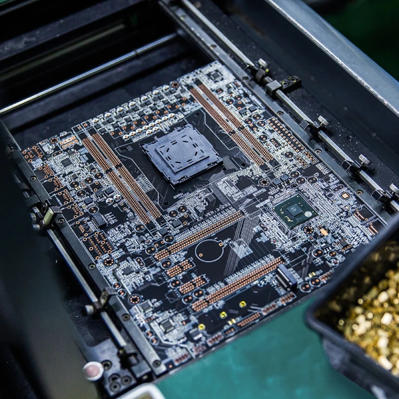
SMT assembly is a method of manufacturing printed circuit boards (PCBs) where electronic components are directly mounted onto the surface of the PCB. Unlike through - hole technology, which requires components to be inserted through holes drilled in the PCB and soldered on the opposite side, SMT components are soldered directly onto the surface pads of the PCB. This approach offers several advantages, such as smaller component size, higher component density, and improved electrical performance, all of which are highly desirable in communication equipment.
In the context of communication devices, such as smartphones, routers, and base stations, the demand for smaller form factors and increased functionality is ever - growing. SMT assembly allows manufacturers to meet these requirements by packing more components into a smaller space. For example, in a modern smartphone, SMT components enable the integration of multiple communication modules, including Wi - Fi, Bluetooth, and cellular connectivity, all within a compact and sleek design.
The SMT Assembly Process for Communication Equipment
The SMT assembly process consists of several key steps, each of which is critical to ensuring the quality and functionality of the final product.
1. PCB Design and Preparation
The first step in the SMT assembly process is the design of the PCB. This involves determining the layout of the components, the routing of the electrical traces, and the placement of the surface pads. For communication equipment, the PCB design must take into account factors such as signal integrity, electromagnetic interference (EMI) shielding, and thermal management.

Once the PCB design is finalized, the bare PCB is manufactured. This typically involves processes such as etching, drilling, and plating to create the necessary electrical connections and physical features on the board.
2. Solder Paste Application
The next step is the application of solder paste onto the surface pads of the PCB. Solder paste is a mixture of tiny solder particles and a flux, which helps to clean the metal surfaces and promote the flow of solder during the soldering process.
The application of solder paste is typically done using a stencil. A stencil is a thin metal or plastic sheet with holes cut out in the shape of the surface pads on the PCB. The stencil is placed over the PCB, and solder paste is spread across the stencil using a squeegee, forcing the paste through the holes and onto the surface pads. For more information on SMT stencil design, you can visit SMT Stencil Design.
3. Component Placement
After the solder paste has been applied, the electronic components are placed onto the surface pads of the PCB. This is done using automated pick - and - place machines, which are capable of accurately placing thousands of components per hour.
The pick - and - place machines use vision systems to identify the components and their orientation, and then pick them up from a feeder and place them onto the correct surface pads on the PCB. In the case of communication equipment, these components may include integrated circuits (ICs), resistors, capacitors, inductors, and antennas.
4. Reflow Soldering
Once the components have been placed, the PCB is passed through a reflow oven. The reflow oven heats the PCB to a temperature high enough to melt the solder paste, creating a permanent electrical and mechanical connection between the components and the PCB.
The reflow process is carefully controlled to ensure that the solder melts evenly and that the components do not overheat or become damaged. This involves precise control of the temperature profile, which includes a pre - heat stage, a soak stage, and a reflow stage.
5. Inspection and Testing
After the reflow soldering process, the assembled PCB is inspected to ensure that there are no soldering defects, such as short circuits, open circuits, or misaligned components. This inspection can be done using automated optical inspection (AOI) systems, which use cameras to capture images of the PCB and compare them to a predefined set of standards.
In addition to visual inspection, the assembled PCB is also tested to ensure that it functions correctly. This may involve functional testing, where the PCB is connected to a test fixture and powered up to verify that it performs its intended communication functions.
Special Considerations for Communication Equipment
Communication equipment has some unique requirements that must be taken into account during the SMT assembly process.
Signal Integrity
In communication devices, maintaining signal integrity is crucial. This means that the electrical signals transmitted between components must be clear and free from distortion. To achieve this, the PCB design must incorporate techniques such as impedance matching, proper trace routing, and EMI shielding.
For example, high - speed signals in communication equipment are often transmitted through microstrip or stripline traces on the PCB. These traces must be designed with the correct impedance to ensure that the signals are transmitted efficiently without reflection or attenuation.
Thermal Management
Communication equipment often generates a significant amount of heat, especially in high - power applications such as base stations. Effective thermal management is essential to prevent overheating and ensure the reliability of the components.
SMT assembly can contribute to thermal management by using components with good thermal properties and by designing the PCB to provide efficient heat dissipation paths. For example, heat sinks can be directly mounted on high - power components using SMT techniques, and thermal vias can be used to transfer heat from the components to the ground plane of the PCB.
Miniaturization
As mentioned earlier, the trend in communication equipment is towards smaller and more compact designs. SMT assembly plays a key role in enabling this miniaturization by allowing for the use of smaller components and higher component densities.
However, miniaturization also poses some challenges, such as increased difficulty in component placement and soldering. To overcome these challenges, advanced assembly techniques and equipment are required, as well as careful component selection and PCB design.
Our Services as an SMT Assembly Supplier
As an SMT assembly supplier, we offer a comprehensive range of services to meet the needs of communication equipment manufacturers.
Prototype and Production Assembly
We provide both prototype and production - scale SMT assembly services. Our state - of - the - art facilities and experienced team of technicians allow us to quickly and efficiently assemble small - batch prototypes for product testing and development. Once the design is finalized, we can scale up production to meet high - volume manufacturing requirements.
Quality Assurance
Quality is our top priority. We have a rigorous quality control system in place to ensure that every assembled PCB meets the highest standards of quality and reliability. This includes in - process inspections at every stage of the assembly process, as well as final testing and inspection before the product is shipped to the customer.
Customized Solutions
We understand that every communication equipment project is unique, with its own set of requirements and challenges. That's why we offer customized SMT assembly solutions tailored to the specific needs of our customers. Whether it's a complex PCB design, a high - performance component selection, or a specialized testing requirement, we have the expertise and flexibility to provide a solution that meets your needs.
To learn more about our SMT PCB assembly services, please visit SMT PCB Assembly. We also offer Mixed Technology PCB Assembly for projects that require a combination of SMT and through - hole components.
Contact Us for SMT Assembly Needs
If you are a communication equipment manufacturer in need of high - quality SMT assembly services, we invite you to contact us. Our team of experts is ready to discuss your project requirements, provide a detailed quote, and work with you to ensure the success of your product development and manufacturing process.
References
- "Surface Mount Technology: Principles and Practice" by C. P. Wong
- "Printed Circuit Board Design: A Practical Guide" by Douglas Brooks
- "Communication Electronics: Principles and Applications" by Louis E. Frenzel Jr.


