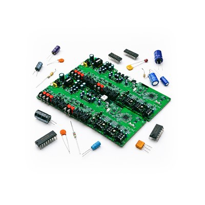
As a provider of PCB assembly services, I've witnessed firsthand the challenges and opportunities that come with managing production waste. In the dynamic world of electronics manufacturing, where precision and efficiency are paramount, waste management is not just a regulatory requirement but a key aspect of sustainable and cost - effective operations.
Understanding the Types of Production Waste in PCB Assembly
In PCB assembly, waste can be broadly categorized into several types. One of the most common forms is physical waste, which includes off - cut materials from PCB boards. When PCBs are fabricated from large panels, the excess material that is trimmed off is considered waste. This can be in the form of small pieces of copper - clad laminate that are no longer usable for the intended PCB design.
Another significant type of waste is related to electronic components. During the assembly process, components may be damaged, misaligned, or simply not fit the requirements. Faulty components such as resistors, capacitors, and integrated circuits are discarded. Additionally, solder waste is a major concern. Excess solder that is used during the soldering process, as well as solder balls that are formed during reflow soldering, contribute to the waste stream.
Chemical waste is also a critical part of the equation. PCB assembly involves the use of various chemicals such as fluxes, solvents, and cleaning agents. These chemicals need to be properly managed as they can be hazardous to the environment and human health if not disposed of correctly.
Strategies for Minimizing Production Waste
Design Optimization
One of the most effective ways to manage production waste is through design optimization. By carefully planning the PCB layout, we can minimize the amount of off - cut material. For example, using panelization techniques to arrange multiple PCBs on a single panel in an efficient manner can significantly reduce waste. This not only saves material costs but also reduces the environmental impact.
Moreover, designing for manufacturability (DFM) is crucial. When the PCB design takes into account the capabilities and limitations of the assembly process, it reduces the likelihood of component errors and rework. For instance, ensuring proper pad sizes and component spacing can prevent misaligned components and soldering issues, which in turn reduces the amount of wasted components.
Component Management
Effective component management is another key strategy. We implement strict inventory control systems to ensure that components are used efficiently. By accurately forecasting the quantity of components needed for each project, we can avoid over - ordering. This not only reduces waste but also saves on inventory costs.
In addition, we have a process for salvaging and reusing components. When a PCB is reworked or scrapped, we carefully inspect the components to see if they can be reused. Components that are still in good condition are tested and then stored for future use. This not only reduces waste but also provides a cost - effective alternative to purchasing new components.


Recycling and Disposal
Recycling is an important part of our waste management strategy. We have established partnerships with certified recycling facilities to ensure that our waste is properly recycled. For example, copper from off - cut PCB materials can be recycled and reused in the manufacturing process. Electronic components can also be recycled to recover valuable metals such as gold, silver, and palladium.
When it comes to chemical waste, we follow strict regulatory guidelines for disposal. We ensure that all chemicals are stored, handled, and disposed of in a safe and environmentally friendly manner. This includes using appropriate containers for chemical storage and working with licensed waste disposal companies.
The Role of Technology in Waste Management
Technology plays a crucial role in managing production waste in PCB assembly. Advanced manufacturing equipment is equipped with sensors and monitoring systems that can detect and correct errors in real - time. For example, automated optical inspection (AOI) systems can quickly identify misaligned components or soldering defects, allowing for immediate rework and reducing the amount of waste generated.
Software tools are also used for waste management. These tools can help in inventory management, production planning, and waste tracking. By using software to analyze production data, we can identify areas where waste can be reduced and implement targeted strategies.
Case Studies
Let's take a look at a couple of case studies to illustrate the effectiveness of our waste management strategies. In one project, we were able to reduce off - cut material waste by 20% through panelization and design optimization. By carefully arranging the PCBs on the panel, we minimized the amount of excess material that was trimmed off.
In another case, we implemented a component salvage program. As a result, we were able to reuse approximately 15% of the components that would have otherwise been discarded. This not only reduced waste but also saved on component costs.
The Business Benefits of Effective Waste Management
Effective waste management in PCB assembly has several business benefits. Firstly, it reduces costs. By minimizing waste, we can save on material costs, inventory costs, and disposal costs. This directly impacts the bottom line and makes our services more competitive in the market.
Secondly, it enhances our reputation. In today's environmentally conscious world, customers are increasingly looking for suppliers who are committed to sustainable practices. By demonstrating our commitment to waste management, we can attract more customers and build long - term relationships.
Finally, it helps us comply with regulatory requirements. There are strict environmental regulations governing the disposal of electronic waste and chemicals. By managing our waste properly, we ensure that we are in full compliance with these regulations, avoiding potential fines and legal issues.
Conclusion
Managing production waste in PCB assembly is a complex but essential task. As a PCB assembly service provider, we are committed to implementing effective waste management strategies. Through design optimization, component management, recycling, and the use of technology, we can minimize waste, reduce costs, and enhance our environmental performance.
If you are in the market for PCB assembly services, we invite you to explore our Turnkey PCB Assembly, Quick‑turn PCB Assembly, and Partial Turnkey PCB Assembly options. We are eager to discuss how we can meet your specific needs and help you achieve your project goals. Contact us to start a conversation about your PCB assembly requirements.
References
- "Electronics Manufacturing Waste Management Best Practices" - Industry report on waste management in electronics manufacturing.
- "Design for Manufacturability in PCB Assembly" - Academic research on optimizing PCB design for efficient manufacturing.
- "Recycling of Electronic Components" - Journal article on the recycling process of electronic components in the PCB assembly industry.