
What is Wave Soldering?
Wave Soldering is a batch soldering process in which a pump creates a stable wave of molten solder in the tin bath, allowing PCB pads and component leads to be soldered instantly as they pass through the wave.
- Scope of Application: Particularly suitable for Wave Soldering for THT Components such as transformers, inductors, and connectors.
- Hybrid Process: Can be combined with reflow soldering - SMT reflow on one side, wave soldering on the other.
- Protective Atmosphere: Nitrogen wave soldering reduces oxidation defects and improves solder joint appearance.
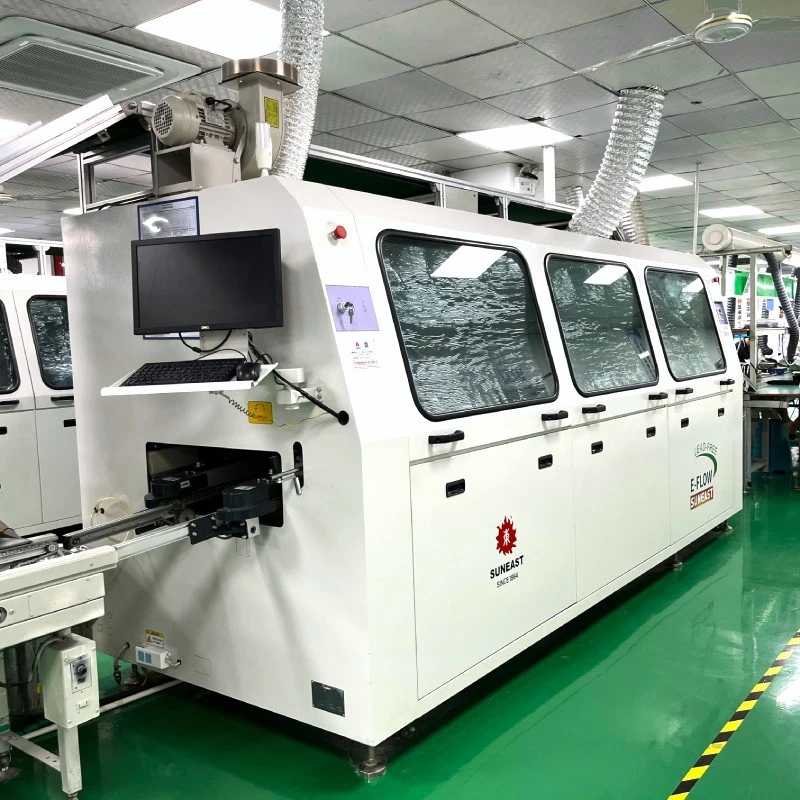
Core Process and Equipment Components
1. Solder Bath and Waveform
- Flat Wave: Ideal for large soldering areas.
- Turbulent Wave: Improves wetting of complex solder joints.
- Temperature Control: Lead-free solder (such as SAC305 for lead free wave soldering) typically requires 260 °C ±5 °C.
2. Equipment Structure
- Conveyor System: Ensures stable PCB transport.
- Flux Application: Spray or foam methods; spray provides more uniform coverage.
- Preheating Zone: 65–121 °C to activate flux and reduce thermal shock.
- Soldering Zone: Solder bath and pump form the wave pattern to complete soldering.
3. Solder Types
- Lead-Containing: Sn63/Pb37, Sn60/Pb40.
- Lead-Free: SAC305, Sn-Cu-Ni.

Critical Process Parameters
Quality Control and Inspection
At STHL, every PCB Wave Soldering process is paired with multiple inspection steps:
- AOI: Checks peripheral solder joint position and solder paste print quality.
- X-ray: Detects hidden defects such as cold joints, bridging, and voids.
- IPC-A-610 Class 3 Compliance: Ensures soldering quality for high-reliability products.

Process Variations and Application Scenarios
- Selective Wave Soldering: Localized soldering for specific joints, ideal for mixed-assembly boards.
- Industrial Control Boards: High-current through-hole component soldering.
- Automotive Electronics: Meets automotive-grade temperature and vibration resistance requirements.
- Home Appliance Main Control Boards: High-efficiency mass production.
- Communications Equipment Backplanes: Multi-pin connector soldering to ensure signal integrity.

Common Defects and Prevention
Voids
Optimize flux application and preheat profile.
Cracks
Control cooling rate.
Insufficient Solder
Adjust wave height and contact time.
Bridging
Optimize PCB layout and solder volume.
Summary and Collaboration Invitation
At STHL, we regard Wave Soldering assembly as a precision manufacturing process - not merely a mass soldering method. If your project requires both efficiency and high reliability in through-hole soldering, or demands consistent, high-quality joints in a lead free wave soldering environment, we welcome the opportunity to discuss process solutions with you.
Send us your design files, and our engineers will optimize manufacturability while our production team ensures delivery quality.
Contact us now: info@pcba-china.com - Let us deliver a high-standard Wave Soldering process that strengthens your product's performance and market competitiveness.
Hot Tags: wave soldering, China wave soldering manufacturers, suppliers, factory, mini wave soldering, Selective Soldering assembly, through hole and surface mount technology, Selective Wave Soldering, Selective Soldering, smt and thru hole technology


