
Why Solder Paste Inspection Is Essential
In SMT production, solder paste printing defects are among the leading causes of poor soldering. If these defects go undetected before placement, the cost of rework rises exponentially - discovering issues after reflow can cost up to ten times more than addressing them at the printing stage, and finding them only during testing can double that again.
The core value of Solder paste inspection lies in:
- Early defect interception: Preventing defective boards from reaching placement and reflow.
- Improved yield: Consistent solder paste deposition directly enhances solder joint reliability.
- Cost reduction: Minimizing rework and scrap, shortening delivery cycles.
- Process optimization: Using inspection data to fine-tune printing parameters and equipment settings.

Inspection Methods and Technical Approaches
1. Automated Solder Paste Inspection
High-resolution optical imaging combined with advanced software algorithms enables fast, consistent inspection of solder paste deposition on every pad, eliminating the fatigue and subjectivity of manual inspection.
2. 2D and 3D Solder Paste Inspection
- 2D: Analyzes solder paste area and position - suitable for basic inspection needs.
- 3D solder paste inspection: Uses structured light or laser to measure solder paste volume, height, and shape. This method detects complex defects such as collapse, excess buildup, and offset, making it the preferred choice for high-density, high-reliability products.
3. Inline Solder Paste Inspection
Integrating the SPI system directly into the SMT production line enables real-time inspection and feedback. When anomalies are detected, the system immediately alerts operators to adjust the printing process, preventing defects from propagating downstream.
SPI Workflow
- Printing – Precisely deposit solder paste onto PCB pads using a stencil.
- Inspection – The PCB passes through the SPI system, capturing 2D or 3D images.
- Analysis – Software measures key parameters such as volume, height, area, and alignment.
- Comparison – Results are compared against pre-set process standards to identify defects.
- Feedback & Adjustment – Real-time feedback is sent to the production line, enabling quick correction of printing parameters.

Key Inspection Metrics and Common Defects
Metrics:
- Volume
- Height
- Area
- Alignment
Common Defects
- Insufficient / excessive solder paste
- Solder bridges
- Misalignment
- Irregular shape
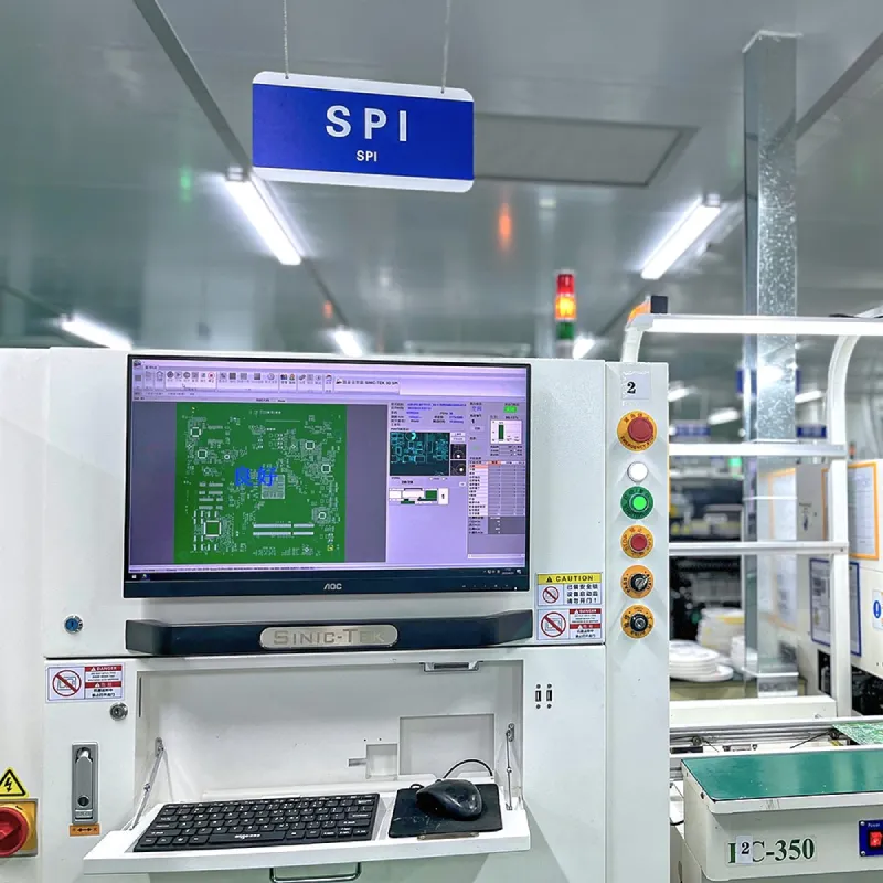
STHL's SPI Capabilities
STHL employs high-precision 3D solder paste inspection systems, integrated with our MES platform for closed-loop traceability of inspection data. Whether through Automated Solder Paste Inspection or Inline Solder Paste Inspection, we can accurately detect defects before placement. Inspection data is correlated with reflow soldering, AOI, X-ray, and other processes to continuously refine parameters, improve yield, and maintain consistent quality.

FAQs
Summary and Invitation for Collaboration
In SMT manufacturing, Solder paste inspection is a vital step for ensuring soldering quality, improving production efficiency, and enhancing customer satisfaction. STHL offers a combined approach of 3D solder paste inspection, Automated Solder Paste Inspection, and Inline Solder Paste Inspection to deliver stable, traceable, and highly consistent inspection capabilities.
If you want to control soldering quality from the source and ensure every PCB reaches the market in peak condition, contact us at info@pcba-china.com.
Hot Tags: solder paste inspection, China solder paste inspection manufacturers, suppliers, factory, PCB In Circuit Test, Inline Solder Paste Inspection, pcb thermal cycling test, System Level Test, Functional Testing, PCB Functional Test


