


Hey there! As a supplier in the SMT PCB Assembly field, I've seen firsthand how crucial a well - designed ground plane is. In this blog, I'm gonna share some tips on how to design a ground plane in SMT PCB Assembly.
Why a Ground Plane is Important
First off, let's talk about why a ground plane matters. A ground plane serves as a reference point for electrical signals on the PCB. It helps reduce electromagnetic interference (EMI), which can cause all sorts of problems like signal distortion and noise. When you've got a proper ground plane, it can also improve the overall performance and reliability of your PCB.
Imagine you're building a high - speed circuit. Without a good ground plane, the signals can bounce around like crazy, leading to errors and malfunctions. But with a well - designed ground plane, it's like having a stable foundation for your electrical signals to travel on.
Design Considerations
Size and Shape
The size and shape of the ground plane are super important. You want to make sure it covers as much of the PCB as possible. A larger ground plane provides a lower impedance path for the return currents, which helps in reducing EMI.
In most cases, a solid ground plane that spans the entire layer is ideal. However, there might be some situations where you need to cut out parts of the ground plane for components or traces. When you do this, make sure the cuts are as small as possible and try to keep them away from high - speed signals.
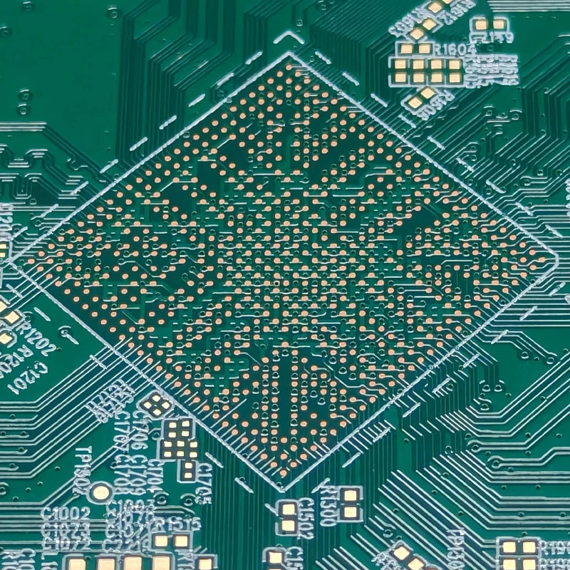
For example, if you're dealing with a SMT BGA Assembly, you might need to cut out some areas of the ground plane to accommodate the BGA package. But you should try to minimize the impact on the overall ground plane integrity.
Clearance and Spacing
Another key factor is the clearance and spacing around the ground plane. You need to maintain a certain distance between the ground plane and other traces or components. This helps prevent short - circuits and ensures proper isolation.
Typically, a clearance of at least 0.2mm is recommended between the ground plane and other conductors. However, for high - voltage or high - speed applications, you might need to increase this clearance.
When designing a SMT PCB Assembly, you also need to consider the spacing between different ground planes if you have multiple layers. Make sure there's enough insulation between them to avoid interference.
Via Placement
Vias are used to connect different layers of the PCB, and their placement can have a big impact on the ground plane design. You want to place vias strategically to ensure a low - impedance connection between the ground planes on different layers.
Avoid placing vias too close to each other, as this can create hotspots and increase the impedance. Also, make sure the vias are properly connected to the ground plane. You can use thermal relief pads or anti - pads to prevent overheating during the soldering process.
Layer Stackup
The layer stackup of the PCB plays a significant role in ground plane design. A well - designed layer stackup can help optimize the performance of the ground plane.
For example, in a multi - layer PCB, you might want to place the ground plane adjacent to a power plane. This creates a capacitor - like effect, which helps in filtering out noise and reducing voltage fluctuations.
If you're working on a Fine Pitch SMT project, a proper layer stackup can also help in routing the fine - pitch traces without causing interference with the ground plane.
Grounding Techniques
There are different grounding techniques you can use in SMT PCB Assembly. One common technique is single - point grounding, where all the ground connections are made at a single point. This helps in reducing ground loops and interference.
Another technique is multi - point grounding, which is suitable for high - frequency applications. In multi - point grounding, the ground connections are made at multiple points on the PCB. This helps in providing a low - impedance path for the high - frequency currents.
Testing and Verification
Once you've designed the ground plane, it's important to test and verify its performance. You can use various tools like an oscilloscope or a network analyzer to measure the impedance and signal integrity of the ground plane.
If you find any issues during the testing, you might need to make some adjustments to the ground plane design. This could involve changing the size, shape, or clearance of the ground plane.
Cost - Effective Design
When designing a ground plane, you also need to consider the cost. You don't want to over - design the ground plane and end up spending more than necessary.

One way to save costs is to use a smaller ground plane if it meets the requirements of your project. You can also use less expensive materials for the ground plane, as long as they provide the necessary performance.
Conclusion
Designing a ground plane in SMT PCB Assembly is a complex but important task. By considering factors like size, shape, clearance, via placement, layer stackup, and grounding techniques, you can create a ground plane that improves the performance and reliability of your PCB.
If you're in the market for SMT PCB Assembly services, I'd love to have a chat with you. Whether you're working on a small project or a large - scale production, we've got the expertise and experience to handle it. Just reach out to us to start a discussion about your specific needs.
References
- Printed Circuit Board Design: A Practical Guide by Andrew Macdonald
- High - Speed Digital Design: A Handbook of Black Magic by Howard Johnson and Martin Graham


