As a seasoned SMT BGA Assembly supplier, I've witnessed firsthand the pivotal role that via design plays in the success of BGA (Ball Grid Array) assemblies. In this blog, I'll delve into the intricacies of via design for SMT BGA Assembly, exploring its significance, key considerations, and best practices.
Understanding Via Design in SMT BGA Assembly
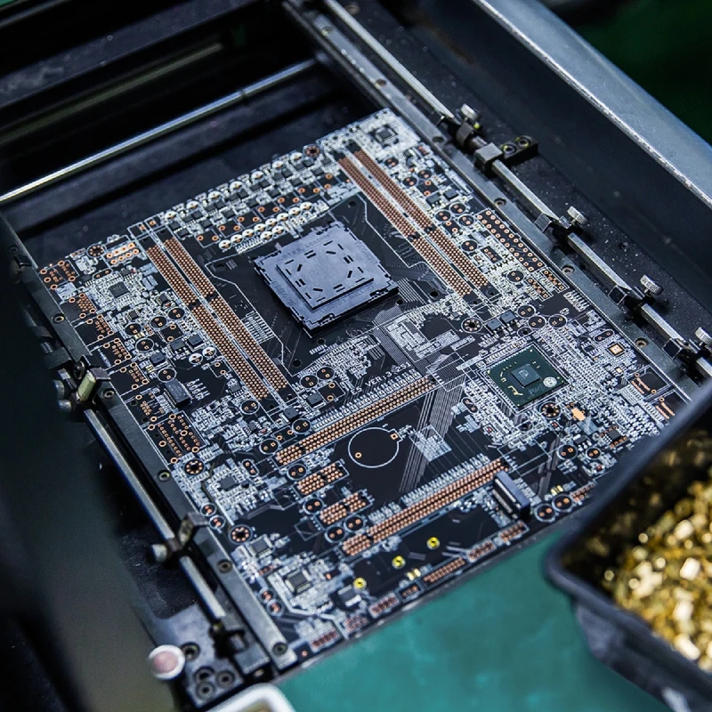
In the realm of SMT BGA Assembly, vias are small holes drilled through the printed circuit board (PCB) that allow electrical connections between different layers. These vias are crucial for routing signals and power between the BGA package and other components on the PCB. The design of these vias can significantly impact the performance, reliability, and manufacturability of the BGA assembly.
Significance of Via Design
- Signal Integrity: Proper via design is essential for maintaining signal integrity. Vias can introduce impedance discontinuities, which can lead to signal reflections and degradation. By carefully designing the vias, we can minimize these effects and ensure that the signals are transmitted accurately and efficiently.
- Power Delivery: Vias also play a vital role in power delivery. They provide a low-resistance path for power to flow from the power source to the BGA package. A well-designed via can help reduce power losses and ensure stable power delivery to the BGA.
- Thermal Management: In addition to electrical considerations, vias can also contribute to thermal management. They can act as heat transfer paths, allowing heat to dissipate from the BGA package to the PCB. This helps prevent overheating and ensures the long-term reliability of the assembly.
Key Considerations in Via Design
- Via Size and Pitch: The size and pitch of the vias are critical factors in via design. The via size should be chosen based on the current carrying capacity and the available space on the PCB. The pitch, or the distance between adjacent vias, should be optimized to minimize interference and ensure proper routing.
- Via Type: There are several types of vias, including through-hole vias, blind vias, and buried vias. Each type has its own advantages and disadvantages, and the choice of via type depends on the specific requirements of the BGA assembly.
- Via Placement: The placement of vias is also important. Vias should be placed as close as possible to the BGA pads to minimize the length of the signal traces. This helps reduce signal loss and improve signal integrity.
- Via Anti-Pad Design: Anti-pads are non-conductive areas around the vias that prevent short circuits. The design of the anti-pads should be carefully considered to ensure that they are large enough to prevent short circuits but not so large that they cause signal degradation.
Best Practices for Via Design
- Use a Design Rule Checker (DRC): A DRC is a software tool that checks the PCB design against a set of predefined rules. By using a DRC, we can ensure that the via design meets the required specifications and standards.
- Optimize Via Routing: The routing of vias should be optimized to minimize the length of the signal traces and reduce the number of vias. This helps improve signal integrity and reduce the risk of signal interference.
- Consider the Manufacturing Process: The via design should take into account the manufacturing process. For example, the size and pitch of the vias should be compatible with the drilling and plating processes used in PCB manufacturing.
- Test and Validate the Design: Before mass production, it is important to test and validate the via design. This can be done through simulation and physical testing to ensure that the design meets the required performance and reliability standards.
Via Design and Mixed Technology PCB Assembly
In Mixed Technology PCB Assembly, which combines surface mount technology (SMT) and through-hole technology (THT), via design becomes even more critical. The vias need to be designed to accommodate both SMT and THT components, and the routing of the vias needs to be carefully planned to ensure proper electrical connections.
Via Design and SMT Stencil Design
The design of the SMT stencil is closely related to the via design. The stencil is used to apply solder paste to the PCB, and the vias need to be properly aligned with the stencil apertures. A well-designed stencil can help ensure that the solder paste is applied accurately and evenly, which is essential for the quality of the BGA assembly. For more information on SMT Stencil Design, please visit our website.
Via Design and High Volume PCB Assembly
In High Volume PCB Assembly, the efficiency and reliability of the via design are crucial. The vias need to be designed to minimize the manufacturing time and cost, while still ensuring the quality and performance of the BGA assembly. By using advanced design techniques and manufacturing processes, we can optimize the via design for high volume production.

Conclusion
Via design is a critical aspect of SMT BGA Assembly. By understanding the significance of via design, considering the key factors, and following the best practices, we can ensure the performance, reliability, and manufacturability of the BGA assembly. As a SMT BGA Assembly supplier, we are committed to providing our customers with high-quality via design solutions that meet their specific requirements.
If you are interested in learning more about our SMT BGA Assembly services or have any questions about via design, please contact us for a consultation. We look forward to working with you to achieve your PCB assembly goals.
References
- Smith, J. (2020). PCB Design for High-Speed Applications. Wiley.
- Johnson, R. (2019). Signal Integrity and Power Integrity Design. Prentice Hall.
- Lee, K. (2018). Advanced PCB Design Techniques. McGraw-Hill.


