


Overview
An NPI build can have a complete set of manufacturing files and still be unready for the SMT line.
That matters when the PCB contains BGA or QFN components. Their solder connections are partly or largely hidden, and small differences in package design can affect the land pattern, stencil apertures, component handling, and inspection strategy.
BGA/QFN assembly readiness means confirming that the selected packages match the released PCB design, the planned manufacturing process is workable, and the first assemblies can be evaluated against agreed requirements.
It doesn't mean every process condition has already been proven. The first build is where some of those assumptions will be tested.
The challenge is deciding which questions need answers before assembly starts and which can reasonably be resolved through a controlled first run.
The First Check Is Physical, Not Administrative
A released BOM and a valid set of Gerber files are useful. Neither proves that the component being supplied matches the footprint on the PCB.
Start with the exact manufacturer part number (MPN).
For a BGA, compare the manufacturer's package drawing with the released PCB land pattern. Ball pitch, package outline, orientation, and the actual ball map all matter. Some arrays have intentionally unpopulated ball positions, so nominal dimensions alone aren't enough to establish a match.
For a QFN, the relevant details include perimeter terminal geometry, package dimensions, Pin 1 identification, and any central exposed pad.
The exposed pad needs particular attention. Its electrical and thermal requirements come from the device documentation. Connecting it to ground simply because that arrangement is common on other QFNs is not a sound design decision.
Some QFN variants also have wettable flanks intended to provide more accessible side solder features. Others do not. That difference can affect both land-pattern design and the inspection method used after assembly.

When the Part Number Changes but the Board Doesn't
Consider a component substitution approved during sourcing.
The replacement may satisfy the electrical requirements, but does it use the same physical package? Does the existing footprint still apply? Have the assembly drawing and placement data been updated?
An approved alternative on the BOM doesn't automatically make it a drop-in assembly replacement.
The manufacturing files must describe the same configuration: approved MPN, package drawing, PCB revision, assembly drawing, and component placement list (CPL).
Orientation is another place where assumptions creep in. A placement-file rotation needs to agree with the component's physical orientation and the conventions used by the machine library. Matching rotation values in different files aren't sufficient proof.
This is an important handoff in a new PCB assembly project.
An EMS engineer can identify a footprint or placement-data conflict during manufacturability review. Any change affecting the OEM's electrical, mechanical, or thermal design still requires the appropriate design approval.
For a prospective STHL project, unclear component variants, package drawings, or PCB revisions can be discussed through info@pcba-china.com with the available engineering files.
The useful outcome isn't merely confirmation that the documents were received. It's agreement on which physical component belongs on which released board.
The Stencil Has to Accommodate Both Packages
Once the package match is clear, attention moves to solder paste printing.
A BGA and a QFN may sit on the same PCB and run through the same SMT line, but their solder connections call for different considerations.
BGA: The Land Pattern Is Only Part of the Interface
The BGA's solder balls, PCB lands, solder-mask openings, and stencil apertures need to form a compatible assembly arrangement.
Solder-mask-defined (SMD) and non-solder-mask-defined (NSMD) land structures have different characteristics. The selected approach should follow the applicable device recommendations and PCB fabrication requirements rather than a generic library preference.
Then there are the vias.
Via-in-pad can be an intentional choice on a densely routed board. Whether it is suitable depends on its construction, fabrication treatment, and relationship to the solder land.
An uncontrolled opening may affect solder behavior during reflow. That doesn't mean every BGA requires the same filling or plating treatment. The actual via design has to be evaluated against the intended assembly process.
Stencil apertures deserve the same scrutiny. Generating them from the CAD paste layer is not, by itself, manufacturing validation.
Before approving the stencil, the team needs a sound basis for the proposed paste deposits and their compatibility with the selected ball and land configuration.
QFN: The Exposed Pad Is a Different Printing Problem
For a QFN with a central exposed pad, the perimeter terminals and center pad may need different paste-deposition strategies.
The exposed pad can provide an important electrical or thermal connection, depending on the device. The amount of solder beneath it can also influence package standoff and the surrounding terminal joints.
Many component manufacturers recommend segmented or windowpane-style apertures for exposed pads to manage solder volume and the conditions associated with void formation.
That approach is common, but not universal.
The appropriate aperture design depends on the specific package, manufacturer guidance, stencil thickness, solder paste, PCB land geometry, and manufacturing process.
Thermal vias can't be left out of that discussion.
A via arrangement may help transfer heat away from the package, yet its construction can also affect solder retention. If solder flows into an unsuitable opening, the intended exposed-pad joint may not form as expected.
The via treatment and central-pad paste pattern therefore need to be considered together.
The exposed-pad design should be reviewed as a whole. Pad geometry, thermal-via construction, stencil apertures, and solder paste deposition affect one another. A change that improves one aspect of the design may introduce a manufacturing constraint elsewhere.
There's no universal exposed-pad paste coverage percentage that applies to every QFN. The same caution applies to void limits and other acceptance criteria: they need an appropriate basis in the component, product application, and agreed requirements.
There is a broader printing constraint, too.
The same stencil may need to serve BGA lands, fine-pitch terminals, small passive components, and the QFN exposed pad. An aperture adjustment that benefits one location isn't necessarily an improvement for the whole board.
Stencil thickness and paste-release characteristics must work across the relevant printing area.
The practical test of a stencil review is whether the proposed design makes sense for the entire assembly, not whether each aperture looks reasonable in isolation.
Actual paste-transfer performance is still something the first print must establish.
A Correct Design Still Needs a Workable SMT Setup
The CAD data may check out. The printer and placement setup are another matter.
Start with the components themselves.
Material presented to the SMT line needs to match the approved part and be suitable for the intended feeding and placement method. Reel or tray presentation, pickup arrangements, and orientation may all affect setup.
Moisture-sensitive handling is another possible constraint.
Where a selected device has applicable moisture sensitivity level (MSL) requirements, its packaging condition, storage, exposure history, and prescribed handling must be considered before reflow.
A matching MPN doesn't automatically establish that an opened package is ready for assembly.
Neither should every BGA or QFN automatically be baked. Handling and any necessary recovery procedure depend on the specific device requirements.
Printer Support Won't Solve Reflow Warpage
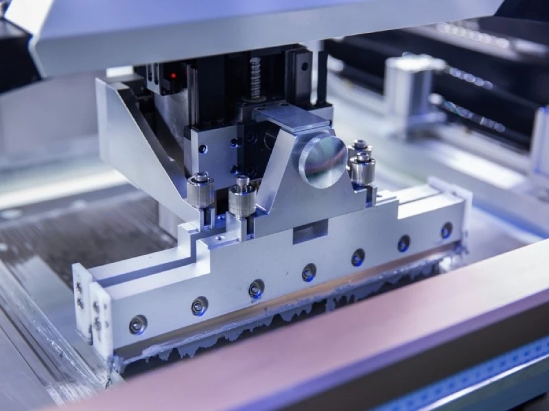
Solder paste printing relies on suitable PCB location, support, and stencil contact.
An inadequately supported area can contribute to board movement or poor stencil contact, particularly where small apertures demand consistent printing conditions.
Panel design, cutouts, board thickness, and available support points all influence the setup.
Double-sided assemblies introduce another complication. During second-side printing, components already mounted underneath may restrict where support tooling can contact the board.
A support arrangement that works on a bare PCB may no longer work once the first side is populated.
That needs to be understood before the board reaches the printer.
But printer support and reflow warpage shouldn't be treated as the same issue.
A well-supported PCB can still experience thermal distortion during reflow. Where the board or package presents a relevant warpage risk, construction, material behavior, handling, and the thermal process may need further review.
One problem concerns how the board is supported during printing or placement. The other concerns how the board and package behave under heat.
An OEM doesn't need to approve every machine setting. It does need to know that the planned manufacturing route can accommodate the actual board and components.
If special support tooling or a particular handling arrangement is necessary, it should be part of manufacturing preparation-not a surprise discovered during the first run.
Inspection Should Answer a Specific Question
Hidden solder connections are one reason BGA and QFN assemblies deserve careful inspection planning.
Still, asking whether the factory has X-ray equipment is only the beginning.
Before the build starts, the OEM and EMS team need to agree on what they intend to inspect, which method can provide useful evidence, and what constitutes an acceptable result.
Different inspection methods answer different questions.
Solder Paste Inspection (SPI) can assess measurable solder paste deposits before placement and reflow, within the capabilities of the inspection system. Depending on the setup, those measurements may include position, area, height, or volume.
That can help establish whether the initial printing results are consistent with the stencil design.
It says nothing directly about the condition of a hidden solder joint after reflow.
Automated Optical Inspection (AOI) can assess visible features such as component presence, orientation, placement, and accessible solder characteristics.
For QFNs, terminal design affects what can be seen.
Wettable flanks can provide more accessible side solder features, making some optical checks more practical. They don't make every solder connection visible, however.
A missing side fillet also shouldn't automatically be treated as a defect when that feature isn't required or expected for the selected package.
X-ray inspection can support evaluation of selected hidden solder features, including BGA ball arrangements, certain bridging conditions, and void patterns. It may also be useful for QFN exposed-pad connections.
The limitations of the imaging method still apply.
A conventional X-ray projection may not reveal every interfacial defect. It doesn't establish electrical performance or long-term reliability by itself, and one void-percentage limit cannot be applied indiscriminately to every package.
Electrical and functional testing cover different ground again.
A functional PASS confirms performance against the procedure and conditions used. It doesn't necessarily establish every hidden-joint or thermal-connection requirement. Equally, acceptable X-ray findings don't prove that the finished circuit will function correctly.
The inspection methods have to match the risks and requirements of the actual product.
Know What an Inconclusive Result Means
Suppose the first X-ray images show a condition that isn't clearly acceptable or unacceptable.
Who makes the call? Is further imaging required? Does the acceptance specification address the feature? Can the affected assemblies proceed, or must they remain on hold?
Those decisions are easier to manage when the inspection scope and disposition authority have been established beforehand.
For the selected BGA and QFN locations, the review needs to identify the intended inspection method, acceptance basis, required coverage, and responsibility for evaluating the findings.
That doesn't imply identical inspection coverage on every project.
Some builds may use selected first-article inspection. Others may have broader requirements because of package risks, application needs, or agreed customer specifications.
The relevant testing and inspection scope should therefore be considered alongside the assembly design-not added after the first boards are complete.
For a new project with sufficient design and manufacturing information available, OEM teams can submit the BOM, Gerber files, CPL, package information, expected quantities, and proposed inspection requirements through the STHL Request for Quotation page.
Shenzhen STHL Technology Co., Ltd. provides PCB assembly and related EMS manufacturing services. The appropriate assembly route, manufacturability review, and inspection requirements are determined in the context of the actual project and agreed responsibilities.
The first-build results will come later. What matters before assembly is having an agreed way to obtain and evaluate them.
Which Open Items Can the First Build Resolve?
NPI work often involves questions that cannot be settled from CAD data alone.
The mistake is treating all open items as either acceptable or unacceptable.
A package mismatch is fundamentally different from a process condition that needs verification on actual assemblies.
If the selected BGA's ball map doesn't match the released PCB land pattern, the underlying manufacturing input needs correction or appropriate resolution.
If the package and PCB match but the first stencil hasn't yet been proven on the printer, the build may be a legitimate way to collect that evidence.
One problem needs a valid input. The other may be the purpose of the engineering trial.
A Trial Is Useful Only When Its Limits Are Clear
A controlled first build may proceed with a known technical question open, provided the proposed activity has a sound basis and the necessary authorization.
That means identifying what is being evaluated, which PCB and component revisions apply, how the trial assemblies will be verified, and who can approve their disposition.
The scope may need to be limited to particular units, operations, or configurations.
Any restrictions on the resulting boards should remain in effect until the relevant requirements have been satisfied.
Completing an SMT run doesn't turn an engineering trial into unrestricted production approval.
Some issues cannot responsibly be left to the first build. If the exact package remains unknown, critical design files conflict, or a required inspection has no workable method or acceptance basis, further review may be necessary before the affected assembly starts.
Permission to Build Is Not Permission to Continue
There are two different decisions.
Pre-build release confirms that the necessary inputs, manufacturing preparations, inspection arrangements, and handling of known issues are sufficient to begin the defined build.
First-article or pilot approval uses actual assembly and verification results to decide whether the project may continue under the agreed requirements.
The first decision allows evidence to be collected. The second evaluates that evidence.
For a more detailed discussion of the subsequent production decision, see STHL's first-article inspection guide.
For BGA/QFN assembly readiness, the immediate question remains whether the intended first build has the right inputs and a credible manufacturing and verification plan.
The First-Build Report Should Settle the Original Question
A useful first-build report doesn't need to document every possible manufacturing detail.
It needs to connect the results to the specific concerns identified before assembly.
If the open issue involved a QFN exposed-pad paste pattern, the team needs relevant evidence about actual paste deposition and the resulting assembly condition.
A general functional PASS won't settle that question on its own.
If the concern involved a BGA package variant, land pattern, or hidden solder feature, the results need to identify the relevant device, board revision, component location, and inspection criteria.

For a double-sided board, the first build may also need to establish whether the planned support arrangement and process sequence worked as intended.
The level of documentation should fit the project and the decision being made.
Relevant records may include stencil and process revisions, SPI measurements, placement verification, X-ray images, test findings, or approved exceptions.
Not every project needs every record.
What matters is whether another qualified engineer can determine which configuration was built, what was checked, what the evidence showed, and what happens next.
Sometimes the result supports continuation. Sometimes it calls for a process adjustment and another controlled evaluation. A design issue may need to return to the OEM for approval.
A first build that reveals a well-defined problem can still be useful. Discovering the issue while the scope is controlled is better than carrying an unexamined assumption into subsequent production.
The sensible release decision is not based on whether everyone expects the first boards to pass.
It's based on whether the manufacturing inputs are correct, the process is workable, and the outstanding questions can be answered with evidence from the build.
That's when a BGA/QFN assembly is ready for its first NPI run.


