


A PCB can be electrically correct, dimensionally correct, and ready for fabrication-and still arrive at the assembly floor in a panel that is difficult to print, support, inspect, or separate.
That is why panelization should not be treated as a final copy-and-paste exercise whose only purpose is to fit more boards into an array.
PCB panelization for SMT assembly defines the temporary workpiece used during solder paste printing, component placement, reflow, inspection, and depaneling.
The panel establishes more than the number of boards per array. It establishes the transport edges, support condition, reference system, step-and-repeat map, product identity, and separation method that downstream equipment and operators will use.
A densely packed panel may look efficient in CAM and still create unnecessary work on the SMT floor.
The practical question is not only:
▎How many boards fit in the panel?
It is:
▎Can the released panel be transported, supported, aligned, inspected, traced, and separated through the intended manufacturing route?
The Assembly Panel Is a Manufacturing Workpiece
The word panel can describe different objects at different stages.
A PCB fabricator may arrange several designs on a larger production panel for imaging, plating, drilling, routing, and other bare-board processes.
The EMS provider is concerned with the workpiece that physically reaches the assembly line. It may be:
- a customer-defined PCB array;
- a panel created by the PCB manufacturer;
- a single PCB with temporary process rails;
- repeated PCB units held within one assembly frame;
- an irregular PCB installed in a removable carrier.
The most material-efficient fabrication layout is not automatically the best assembly workpiece.
An assembly-ready panel also needs to account for:
- transport and clamping;
- underside support;
- PCB-unit orientation;
- fiducial strategy;
- machine-program preparation;
- inspection mapping;
- unit-level traceability;
- testing and downstream handling;
- the intended depaneling method.
A panel is not assembly-ready merely because its Gerber data can be fabricated.
Can the Panel Be Transported and Supported?
The first engineering question is mechanical.
Can the panel move through the intended printer, conveyors, placement equipment, reflow oven, solder paste inspection system, AOI equipment, and downstream stations without interference or unstable handling?
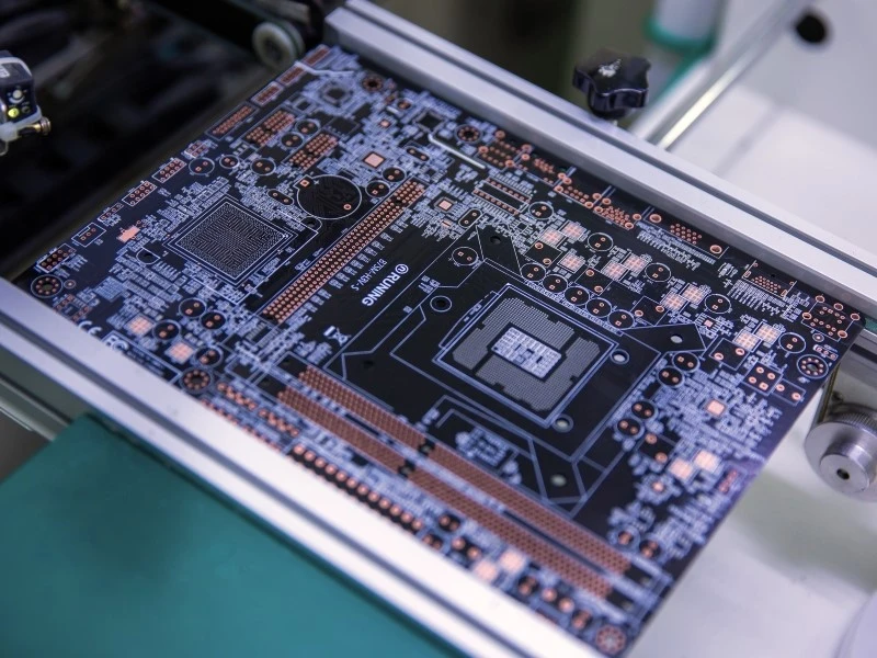
Transport Edges Must Match the Actual Route
Temporary process rails may provide:
- conveyor contact;
- clamping clearance;
- additional rigidity;
- space for fiducials;
- identification or traceability space;
- safer manual handling.
Their dimensions and locations depend on the actual equipment and project.
A single rail width cannot be applied to every SMT line because the answer changes with:
- transport direction;
- conveyor and clamp geometry;
- component overhang;
- PCB thickness;
- single- or double-sided assembly;
- panel rigidity;
- downstream separation.
A rail that works in the solder paste printer may still interfere with a later station.
Adding more border material is not automatically safer.
A process rail is useful only when it supports the complete manufacturing route.
Printing Depends on Contact and Backside Support
Solder paste printing requires repeatable contact between the stencil and PCB surface.
The printer must locate, clamp, and support the panel without contacting unsuitable bottom-side features.
Panel design can affect that condition through:
- large routed openings;
- narrow connecting tabs;
- thin PCB construction;
- irregular outlines;
- weak internal support;
- bottom-side components;
- labels or solder joints beneath the support area;
- openings that restrict backup-tooling locations.
Printers typically use backup pins or dedicated support tooling to hold the panel flat during solder paste printing. Placement equipment may also use support pins to limit vertical movement while components are placed.
In both cases, the support layout needs to be checked against bottom-side components, solder joints, labels, routed openings, and any other features that cannot safely carry load.
The printer does not care how elegant the nesting looks. It cares whether the panel can be clamped and supported consistently.
A large panel is not automatically unstable.
A small panel is not automatically easy to print.
The question is whether the released array can be supported in the actual equipment.
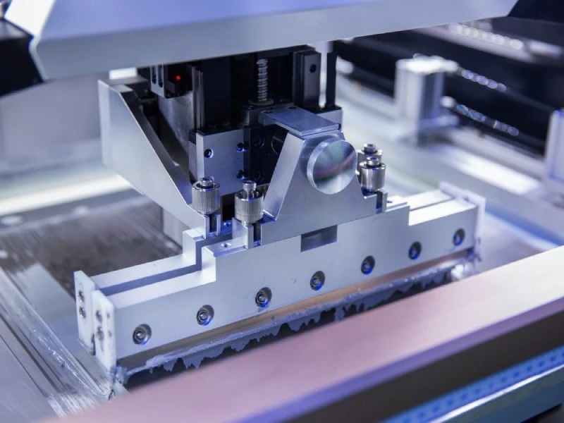
Can the Machines Locate Every PCB Unit Correctly?
Once the panel reaches the line, the physical workpiece must match the manufacturing data.
A centroid or pick-and-place file normally identifies component coordinates and rotations on the PCB. The production program then has to connect those coordinates to:
- the panel origin;
- each PCB-unit origin;
- step-and-repeat offsets;
- unit rotations;
- panel and local fiducials;
- product variants;
- known bad boards;
- the released placement data.
Global and Local Fiducials Have Different Roles
Panel-level fiducials help the equipment establish the position and orientation of the complete array.
Local fiducials may provide additional registration for an individual PCB unit or a placement-sensitive area.
Whether local fiducials are required depends on:
- component pitch and package;
- panel dimensions;
- PCB distortion;
- placement-accuracy requirements;
- available board features;
- machine-recognition strategy;
- the receiving factory's process standard.
There is no single fiducial count or diameter that should be copied into every panel drawing without confirming the assembler's equipment and process.
The reference mark also needs to be on a stable part of the panel.
A fiducial located on a flexible breakaway tab is a weak reference because the feature can move independently of the PCB units it is intended to locate.
Mixed Orientation Is a Tradeoff
Rotating alternate PCB units can improve panel utilization.
That does not make the panel wrong. Modern placement and inspection equipment can process rotated units when the released data and machine programs are prepared correctly.
The tradeoff is additional work in:
- coordinate transformation;
- polarity verification;
- first-article review;
- inspection mapping;
- operator instructions;
- variant control;
- depaneling guidance.
For one simple and stable product, the additional work may be minor.
For mixed revisions, programmed devices, polarized components, or frequent engineering changes, consistent orientation can reduce unnecessary interpretation.
A mixed-orientation array is not automatically a manufacturing problem. It simply requires more disciplined data control and verification.
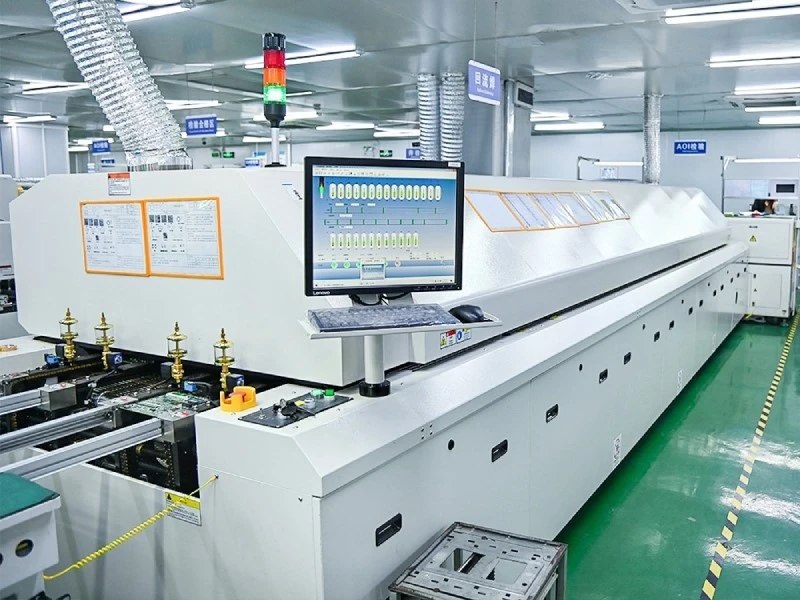
The Panel Becomes a Heated Mechanical Structure
During reflow, the panel is transported and heated as a populated mechanical structure.
Its behavior may be influenced by:
- PCB thickness;
- panel dimensions and aspect ratio;
- routed openings;
- rail construction;
- copper distribution;
- component mass;
- PCB-unit orientation;
- transport and support conditions.
These factors can contribute to bowing, twisting, or changes in how the panel sits during the thermal cycle.
They do not create one universal maximum panel size, nor do they independently explain every solder defect.
Tombstoning, bridging, opens, and head-in-pillow can involve several interacting factors, including:
- stencil design;
- solder paste condition and volume;
- pad geometry;
- solder-mask design;
- component termination;
- placement;
- package warpage;
- wetting behavior;
- thermal profile.
A flexible or poorly supported panel may deserve investigation.
It should not become the automatic root cause simply because a defect appeared after reflow.
Panelization changes the process conditions. Root cause still has to follow the evidence.
Inspection Depends on a Controlled PCB-Unit Map
Panelized production works well when the inspection program and the physical array describe the same released product condition.
SPI and AOI may need controlled information about:
- panel origin;
- PCB-unit positions;
- step-and-repeat offsets;
- unit orientation;
- fiducial strategy;
- component coordinates;
- DNP rules;
- product variants;
- known bad boards;
- panel ID and unit-level traceability.
A repeated array can simplify inspection-program preparation when every unit follows the same released data.
The work becomes more complicated when one panel contains:
- different products;
- different revisions;
- alternating rotations;
- mixed population rules;
- unclear bad-board markings;
- customer-specific variants.
The equipment may be capable of handling that variation.
The variation still needs to be defined before the program is approved.
Bad-Board Handling Must Be Agreed
A PCB manufacturer may identify one defective PCB unit within an otherwise usable panel.
The SMT process then needs an agreed rule for:
- how the bad unit is marked;
- whether solder paste is printed on it;
- whether component placement skips it;
- how the inspection program records it;
- whether the panel remains acceptable;
- how the final usable quantity is reconciled.
The exact marking and skip method depend on the factory, equipment, and project.
A handwritten assumption discovered during line setup is not a controlled bad-board process.
Panelization Affects X-Ray Traceability, Not X-Ray Capability
Panelization helps associate an inspected BGA, LGA, QFN, or other hidden-joint package with:
- the correct PCB unit;
- its position within the panel;
- the component reference;
- the production lot;
- the inspection record.
It does not determine X-ray penetration, image contrast, or defect-detection capability by itself.
Those depend on the package, PCB construction, inspection equipment, imaging setup, and agreed inspection method.
The panel helps preserve location and identity. It does not replace the X-ray inspection plan.
Panel-Level AOI Cannot See Damage Created Later
When AOI is completed before depaneling, it confirms the visible assembly condition at that point in the process.
It cannot confirm whether the later separation step introduces:
- board-edge damage;
- excessive tab remnants;
- mechanical strain;
- disturbed connectors;
- cracked components;
- damage to solder joints near the separation area.
A post-depanel visual check can identify board-edge damage, obvious handling damage, disturbed components, and unacceptable tab remnants.
It cannot, by itself, prove that mechanically sensitive components are free from latent cracking.
Any additional inspection should follow the product risk, component location, separation method, and customer requirements.
AOI can only inspect the condition presented to it. It cannot inspect damage that has not happened yet.
Can the Boards Be Separated Without Adding Risk?
Depaneling occurs after the components and solder joints are already present.
That makes separation part of assembly risk, not merely a bare-board fabrication feature.
Common approaches include:
- V-scoring;
- routed tabs;
- mouse-bite perforations;
- mechanical routing;
- removable carriers;
- other project-specific separation methods.
V-Scoring and Routed Tabs Suit Different Board Geometries
V-scoring is generally suited to continuous straight separation lines and compatible PCB outlines.
Routed tabs provide greater flexibility for:
- irregular outlines;
- local cutouts;
- curved profiles;
- selected retention points;
- edge features that prevent continuous scoring.
Neither method is universally safer or less expensive.
The choice depends on:
- PCB outline;
- board thickness;
- required edge condition;
- component location;
- panel rigidity;
- separation equipment;
- acceptable mechanical loading;
- enclosure fit after separation.
V-scoring may provide a dense, straightforward array for compatible rectangular boards.
Routed tabs may offer better geometric flexibility, but they can leave tab remnants, require local cleanup, or apply separation force through specific retention points.
The method should be selected for the actual board and depaneling process, not because one option is generally considered better.
Sensitive Components Need a Method-Specific Review
Components close to a score line or breakout tab may be exposed to PCB bending or localized separation force.
The risk depends on more than distance alone:
- package type;
- component orientation;
- copper and routing around the component;
- PCB thickness;
- tab location;
- separation direction;
- manual or automated depaneling.
Ceramic capacitors and other mechanically sensitive components deserve particular attention because PCB bending can transfer stress into the component body, termination, or nearby solder joint.
There is no universal component-to-score or component-to-tab distance that can be applied without considering the actual construction and process.
Depaneling begins after the normal SMT process appears complete. Poor separation planning can create a new problem at the final mechanical step.
What Panelization Influences-and What It Does Not Decide
|
Panel decision |
What it can influence |
What it does not decide by itself |
|
Panel dimensions and rails |
Transport, clamping, support, and equipment compatibility |
Universal throughput or yield |
|
Fiducial strategy |
Registration, orientation, and coordinate mapping |
Placement quality without correct data and setup |
|
PCB-unit orientation |
Programming, polarity review, and inspection mapping |
Whether rotated boards are inherently defective |
|
Rigidity and support access |
Printing and placement stability |
The root cause of every solder defect |
|
Bad-board marking |
Skip logic, inspection records, and quantity reconciliation |
Bare-board acceptance criteria |
|
V-score lines or routed tabs |
Panel retention, edge condition, and separation method |
One universal component keep-out distance |
|
Panel ID and unit markings |
Traceability before and after separation |
The complete inspection plan |
|
Tooling features |
Fixture and handling compatibility where required |
A mandatory feature for every product |
Panelization is an engineering input.
It is not a universal explanation for every downstream problem.
The Densest Panel Is Not Always the Lowest-Cost Panel
Placing more PCB units into one array may improve bare-board utilization and reduce individual-board handling.
The same layout may also require:
- more complicated support planning;
- mixed-orientation programming;
- additional first-article verification;
- more complex inspection mapping;
- a less convenient depaneling route;
- additional manual identification;
- tighter handling instructions.
That does not make dense panelization wrong.
The awkward panel is rarely the one that fails at the first machine. It is the one that needs a different workaround at every station.
A slightly less dense array may be the better choice when it provides:
- stable transport;
- simpler programming;
- clearer unit identity;
- safer underside support;
- more controlled separation;
- fewer exceptional work instructions.
The decision should therefore consider the complete manufacturing route, not only bare-board utilization.
Control the Panel Revision Before Releasing Stencils and Programs
A panel drawing should be controlled like any other manufacturing document.
Once downstream preparation has begun, a change to the panel may affect:
- stencil fabrication data;
- printer setup;
- panel and PCB-unit origins;
- step-and-repeat offsets;
- placement programs;
- SPI and AOI programs;
- carriers or fixtures;
- bad-board skip logic;
- serial-number mapping;
- depaneling setup.
Changes that look minor in CAM may not be minor to the assembly team.
Moving a fiducial, rotating one PCB unit, changing the panel origin, adding a rail, or relocating a breakout tab may invalidate downstream assumptions.
A panel revision mismatch can cause more disruption than the original geometry issue.
The PCB fabricator, stencil supplier, SMT programmer, inspection engineer, and depaneling team need to work from the same released panel revision.
The panel should not be corrected independently by different departments after tooling and programs have already been prepared.
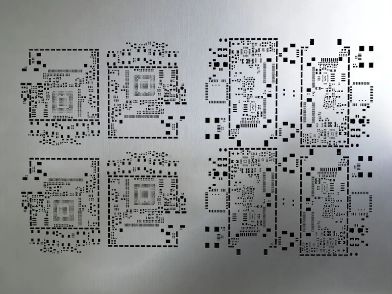
What OEM Buyers Should Provide for Panel Review
A useful review package normally includes the available:
- Gerber, ODB++, IPC-2581, or equivalent fabrication data;
- drill data and final PCB outline;
- PCB thickness and material requirements;
- centroid or pick-and-place file;
- assembly drawing;
- top- and bottom-side assembly information;
- bottom-side components and component overhangs;
- edge-sensitive or mechanically sensitive components;
- customer-defined orientation or panel dimensions, where applicable;
- traceability, serial-number, test, and fixture requirements;
- depaneling restrictions;
- current product revision.
Where an array has already been created, the panel drawing should identify:
- panel outer dimensions;
- units per panel;
- PCB-unit orientation;
- panel origin and PCB-unit origins;
- process rails;
- global and local fiducials;
- tooling features where required;
- board-to-board spacing;
- V-score lines, routed tabs, or mouse-bite locations;
- bad-board identification;
- panel and unit-level markings.
The goal is not to send the largest possible file package.
It is to ensure that PCB fabrication, stencil preparation, SMT programming, inspection, and depaneling are reviewing the same released condition.
What OEM Buyers Should Confirm Before Panel Release
Before approving the panel, confirm:
- Does the panel fit the intended printing, placement, reflow, and inspection route?
- Are its handling edges and underside support areas compatible with the equipment?
- Are panel and local fiducials defined for the receiving factory?
- Are all PCB-unit origins, step-and-repeat offsets, and rotations represented correctly?
- How are defective units marked, skipped, and reconciled?
- Will testing occur at panel level or after depaneling?
- Have the separation method and sensitive edge components been reviewed together?
- How will unit-level product and lot traceability be preserved after depaneling?
- Which released panel revision governs stencil fabrication, machine programming, fixture preparation, and inspection setup?
These questions should be answered before the stencil, placement program, inspection program, fixture, and depaneling setup have already been committed.
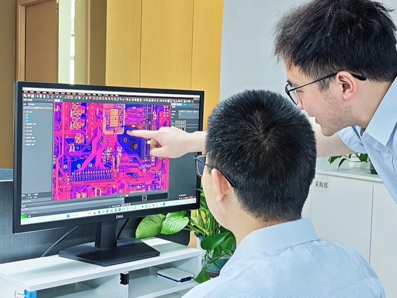
How STHL Reviews PCB Panelization for SMT Production
Shenzhen STHL Technology Co., Ltd. supports PCB fabrication, PCB assembly, and engineering preparation within a coordinated EMS manufacturing workflow.
Within the confirmed project scope, a panelization review may consider:
- board outline and panel dimensions;
- units per panel;
- PCB-unit orientation;
- transport rails and handling edges;
- fiducial and coordinate strategy;
- underside support restrictions;
- stencil-printing preparation;
- placement-data alignment;
- inspection-program implications;
- bad-board handling;
- V-score or routed-tab arrangement;
- components near separation areas;
- unit-level traceability after depaneling;
- panel revision consistency.
The purpose is not to impose one standard array on every PCB.
It is to confirm that the released panel is compatible with the intended fabrication, PCB assembly, inspection, and separation route.
Review STHL's PCB Manufacturing capabilities when PCB fabrication, panelization, and downstream assembly preparation need to be coordinated.
Submit the available fabrication and assembly data through Request a Quote, or send the project requirements to info@pcba-china.com.
Conclusion
PCB panelization affects SMT assembly because the production line handles the array as a physical workpiece and coordinate map.
It influences:
- transport and support;
- stencil contact;
- placement registration;
- PCB-unit orientation and offsets;
- SPI and AOI programming;
- bad-board handling;
- unit-level traceability;
- depaneling conditions.
It does not replace good PCB design, stencil design, reflow profiling, inspection planning, test development, or evidence-based failure analysis.
The right panel is not simply the one that fits the most boards. It is the one that moves through printing, placement, reflow, inspection, and separation without creating avoidable exceptions.
That is why panelization should be reviewed and revision-controlled before stencils, machine programs, inspection programs, fixtures, and depaneling setups are released.


