


Solder voids are a common issue in wave soldering, which can significantly affect the quality and reliability of printed circuit board (PCB) assemblies. As a wave soldering supplier, we understand the importance of detecting these voids accurately and efficiently. In this blog, we will explore various methods to detect solder voids in wave soldering and discuss their advantages and limitations.
Understanding Solder Voids in Wave Soldering
Before delving into the detection methods, it's essential to understand what solder voids are and why they occur. Solder voids are small pockets of air or gas trapped within the solder joint during the soldering process. They can be caused by several factors, including improper flux application, insufficient preheating, high soldering temperature, and contaminants on the PCB or components.
Solder voids can lead to a range of problems, such as reduced mechanical strength, poor electrical conductivity, and increased susceptibility to thermal stress. Therefore, detecting and eliminating these voids is crucial to ensure the long - term performance and reliability of PCB assemblies.
Visual Inspection
Visual inspection is the most basic and commonly used method for detecting solder voids. It involves using a magnifying glass or a microscope to examine the solder joints on the PCB. This method is relatively simple and cost - effective, making it suitable for small - scale production or initial quality checks.
During visual inspection, trained operators look for signs of voids, such as irregularities in the solder surface, dark spots, or bubbles. However, visual inspection has its limitations. It can only detect relatively large voids that are visible to the naked eye or under low - magnification. Smaller voids, which may still have a significant impact on the performance of the solder joint, can easily be missed.
X - Ray Inspection
X - ray inspection is a more advanced method for detecting solder voids. It uses X - rays to penetrate the PCB and components, allowing for a detailed view of the internal structure of the solder joints. X - ray inspection can detect both surface and internal voids, regardless of their size.
There are two main types of X - ray inspection: 2D and 3D. 2D X - ray inspection provides a flat image of the PCB, which can be used to identify voids in the solder joints. However, it may not be able to accurately determine the depth and size of the voids. 3D X - ray inspection, on the other hand, provides a three - dimensional image of the PCB, allowing for more precise measurement and analysis of the voids.
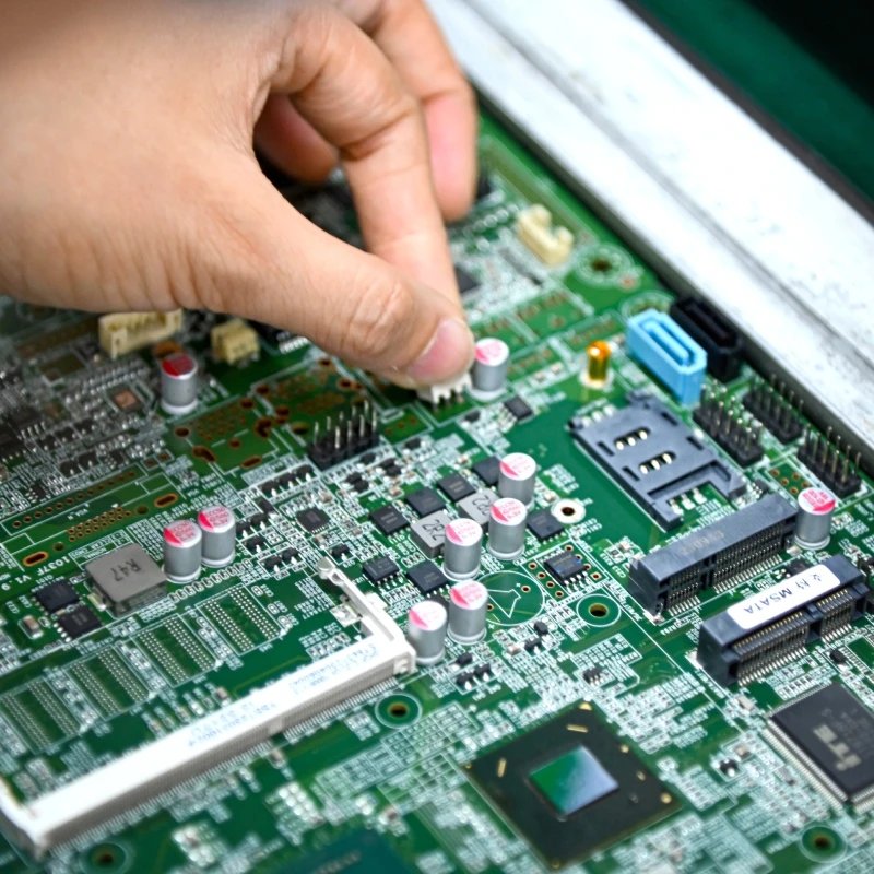

The advantage of X - ray inspection is its high accuracy and ability to detect hidden voids. However, it is also a relatively expensive method, requiring specialized equipment and trained operators. Additionally, X - rays can be harmful to human health, so proper safety measures must be taken.
Automated Optical Inspection (AOI)
Automated Optical Inspection (AOI) is another popular method for detecting solder voids. AOI systems use cameras and image - processing algorithms to inspect the solder joints on the PCB. They can quickly and accurately detect a wide range of soldering defects, including voids.
AOI systems work by comparing the actual image of the solder joint with a pre - defined reference image. Any deviations from the reference image are flagged as potential defects. AOI can detect both surface and near - surface voids, and it can be integrated into the production line for real - time inspection.
The main advantage of AOI is its high speed and efficiency. It can inspect a large number of PCBs in a short period of time, reducing the production cycle and improving productivity. However, AOI has limitations in detecting internal voids, as it only relies on surface images.
Ultrasonic Inspection
Ultrasonic inspection is a non - destructive testing method that uses high - frequency sound waves to detect solder voids. When an ultrasonic wave is applied to the solder joint, it is reflected differently depending on the presence of voids. By analyzing the reflected waves, it is possible to identify the location and size of the voids.
Ultrasonic inspection can detect both surface and internal voids, and it is particularly effective for detecting small voids that may be missed by other methods. However, it requires specialized equipment and trained operators, and it may not be suitable for all types of PCB assemblies.
Thermal Imaging
Thermal imaging is a method that uses infrared cameras to detect solder voids. When a current is passed through the PCB, the solder joints with voids will have a different temperature distribution compared to the normal joints. By analyzing the thermal image, it is possible to identify the locations of the voids.
Thermal imaging is a non - contact method, which means it does not damage the PCB or components. It can also detect voids in real - time during the soldering process. However, it may be affected by external factors such as ambient temperature and the presence of other heat sources.
Choosing the Right Detection Method
When choosing a method to detect solder voids in wave soldering, several factors need to be considered. These include the size and type of the voids, the production volume, the cost, and the level of accuracy required.
For small - scale production or initial quality checks, visual inspection may be sufficient. However, for large - scale production or high - reliability applications, more advanced methods such as X - ray inspection or AOI may be necessary.
It's also important to note that no single method can detect all types of solder voids. Therefore, a combination of different methods may be used to achieve the highest level of detection accuracy.
Our Services as a Wave Soldering Supplier
As a wave soldering supplier, we offer a comprehensive range of services to help our customers detect and eliminate solder voids. We have state - of - the - art inspection equipment, including X - ray machines, AOI systems, and ultrasonic inspection devices. Our experienced technicians are trained to use these tools effectively to ensure the highest quality of solder joints.
In addition to inspection services, we also provide technical support and advice on wave soldering processes. We can help our customers optimize their soldering parameters, such as preheating temperature, soldering time, and flux application, to reduce the occurrence of solder voids.
We also offer Manual Through Hole Assembly, DIP Assembly, and Selective Soldering services, which can be customized to meet the specific needs of our customers.
Contact Us for Procurement and Consultation
If you are interested in our wave soldering services or need more information about detecting solder voids, please feel free to contact us. Our sales team is ready to discuss your requirements and provide you with a detailed quotation. We are committed to providing high - quality products and services to our customers and look forward to working with you.
References
- "Fundamentals of Wave Soldering" by John Doe
- "Inspection Techniques for PCB Assemblies" by Jane Smith
- "Non - Destructive Testing in Electronics Manufacturing" by Robert Johnson


